제품 설명:
통신 PCB 어셈블리는 현대 통신 인프라의 엄격한 요구 사항을 충족하도록 설계된 고도로 진보되고 신뢰할 수있는 솔루션입니다.이 제품은 뛰어난 제작 품질로 돋보인다.가장 까다로운 환경에서도 최적의 성능을 보장하기 위해 최첨단 재료와 제조 기술을 통합합니다.이 집합은 강력한 통신 기능을 필요로 하는 응용 프로그램에 이상적입니다..
이 커뮤니케이션 PCB 조립체의 결정적인 특징 중 하나는 표면 마무리 옵션입니다.그것은 ENIG (Electroless 니켈 몰입 금) 및 HASL (고온 공기 용접 평준화) 납 없는 완공과 함께 제공됩니다., 이는 우수한 용접성과 산화 및 진열에 대한 우수한 보호를 제공합니다.평평한 표면과 고주파 통신 회로에서 신뢰할 수있는 성능으로 잘 알려져 있습니다., 그것은 고급 HDI PCB 애플리케이션에 대한 완벽한 선택입니다.HASL 납 없는 완공은 우수한 기계적 및 전기적 특성을 유지하면서 환경 표준을 준수합니다..
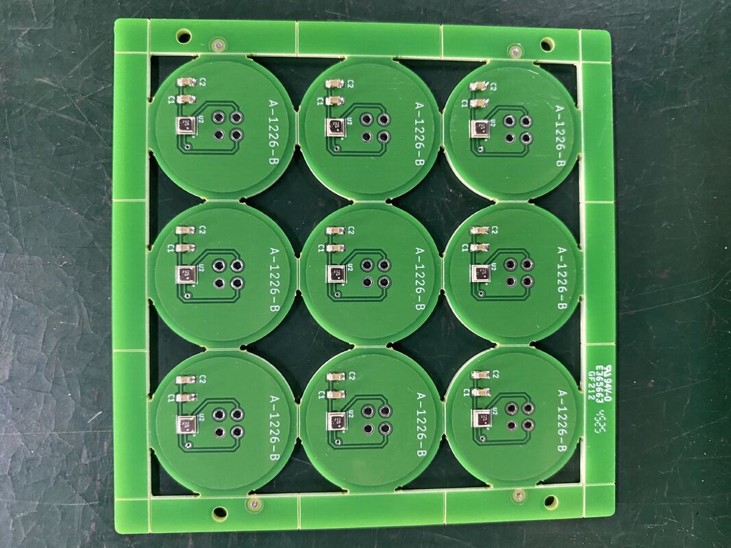
집합은 0.1mm의 최소 구멍 지름을 지원하여 현대 통신 장치에서 필수적인 고밀도 상호 연결을 만들 수 있습니다.이 정밀 굴착 능력은 복잡한 회로 설계의 통합을 가능하게 하고 통신 인프라 하드웨어의 소형화 추세를 지원합니다.작은 구멍 지름, 첨단 PCB 제조 기술과 결합,신호 무결성이나 기계적 강도를 손상시키지 않고 집합이 복잡한 라우팅 및 계층 요구 사항을 수용 할 수 있음을 보장합니다..
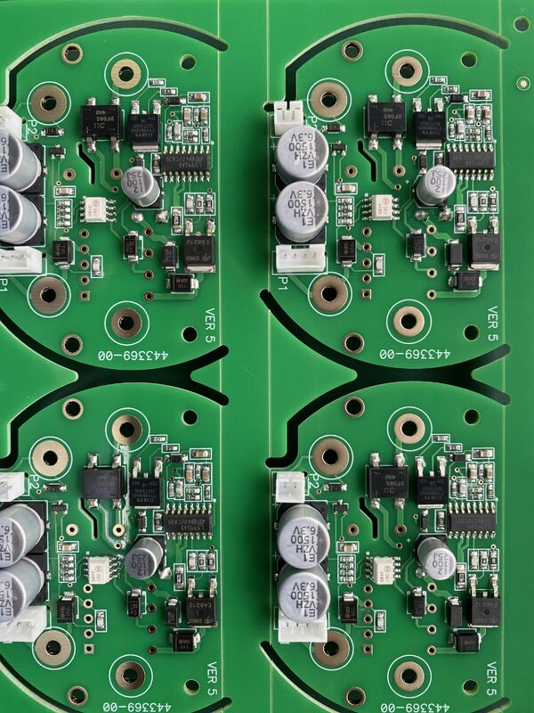
또한이 제품은 구멍, 블라인드 및 묻힌 비아스를 포함한 다재다능한 비아 유형을 갖추고 있습니다. 이러한 비아 유형은 HDI PCB 설계에서 중요합니다.그들은 다층 연결을 촉진하고 보드의 전반적인 전기 성능을 향상시키기 때문에구멍 뚫린 비아스는 견고한 기계적 연결을 제공하며 강한 용접 관절이 필요한 부품에 이상적입니다.맹인 비아스는 전체 보드를 통과하지 않고 외부 층과 내부 층을 연결합니다, 따라서 공간을 절약하고 신호 경로 길이를 줄입니다. 묻힌 비아스는 내부 계층만을 연결하여 보드 레이아웃을 더욱 최적화하고 더 높은 회로 밀도를 허용합니다.이 조합은 통신 PCB 조립을 통해 우수한 신호 무결성과 신뢰성을 제공할 수 있습니다., 통신 인프라 시스템 내의 무거운 전류 애플리케이션에 필수적입니다.
이 집합의 보드 두께는 0.2mm에서 6mm까지 다양하며 다양한 응용 요구 사항에 맞게 유연성을 제공합니다. 더 얇은 보드는 컴팩트하고 가벼운 장치에 이상적입니다.두꺼운 보드가 더 높은 내구성을 제공하고 무거운 전류 부하를 지원하는 동안두께 선택의 폭이 넓어짐에 따라 집합체는 특정 기계 및 전기 요구 사항을 충족시킬 수 있습니다.통신 인프라 프로젝트의 광범위한 스펙트럼에 적합하도록.
이 제품의 핵심은 HDI PCB 기술입니다. HDI PCB는 고밀도 상호 연결 인쇄 회로 보드를 의미합니다. HDI PCB는 뛰어난 회로 밀도로 알려져 있습니다.전기 성능 향상이 통신 PCB 어셈블리에서 HDI 기술을 사용하는 것은 복잡한 회로를 컴팩트한 형태 요소로 통합 할 수 있습니다.더 빠른 신호 전송과 낮은 전력 소비를 가능하게 합니다이는 특히 효율적인 데이터 전송과 신뢰할 수있는 중류 처리가 가장 중요한 통신 인프라에서 중요합니다.
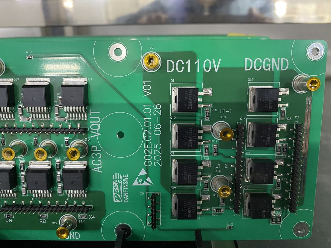
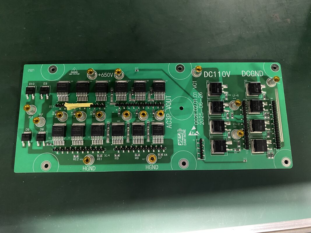
무거운 전류 응용의 엄격한 조건에 견딜 수 있도록 설계 된 이 집합은 통신 인프라 시스템에서 안정적이고 중단되지 않은 작동을 보장합니다.성능 또는 신뢰성 저하 없이 무거운 전류 부하를 처리 할 수있는 능력은 전력집약적인 통신 장비에 필수적인 구성 요소가됩니다.기본 스테이션, 네트워크 라우터, 또는 다른 중요한 인프라 구성 요소에 사용 여부,이 통신 PCB 조립은 원활한 연결을 유지하기 위해 필요한 신뢰할 수있는 성능을 제공합니다.
요약하자면, 통신 PCB 조립은 ENIG와 HASL와 같은 고급 표면 마무리 옵션을 결합한 최첨단 솔루션입니다.뚫린 구멍을 포함한 종류를 통해 다재다능합니다, 맹인, 그리고 묻힌, 그리고 0.2mm에서 6mm의 넓은 보드 두께 범위.통신 인프라 내의 무거운 전류 요구 사항을 지원하도록 특별히 설계되었습니다., 탁월한 신뢰성, 내구성, 전기 성능을 제공합니다.이것은 현대 통신 시스템의 까다로운 과제를 충족 할 수있는 고품질 PCB 조립체를 찾는 엔지니어와 제조업체에게 이상적인 선택이됩니다..
특징:
- 제품명: 통신 PCB 조립
- 제조사: 높은 품질 표준을 보장하는 신뢰할 수 있고 경험이 많은 제조사
- PCB 층: 복잡한 회로 설계에 필요한 6 층
- 임페던스 제어: 네, 최적의 신호 무결성을 위해
- 판 두께: 0.2-6mm 다양한 응용 요구 사항에 적합
- 두꺼운 구리: 무거운 전류 용량을 지원하고 내구성을 향상시킵니다
- 전압 보호: 민감한 통신 부품을 보호하기 위해 통합
- 외부 패키지: 안전하고 안전한 운송을 위한 카튼 포장
기술 매개 변수:
| 제품 이름 |
통신 PCB 조립 |
| 비타이프 |
구멍 을 뚫고, 장님 이 되어 묻혔다 |
| 맞춤형 |
그래요 |
| 표면 가공 |
ENIG, HASL 납 없는 |
| 적용 분야 |
5G 통신 |
| 판 두께 |
0.2-6mm |
| 임페던스 제어 |
그래요 |
| 구멍 지름 미니 |
00.1mm |
| 통신 PCB |
높은 Tg170 및 높은 Tg180 |
| 외부 패키지 |
팩 |
응용 프로그램:
통신 PCB 어셈블리는 강력한 통신 인프라 애플리케이션을 위해 특별히 설계된 필수 부품입니다. 사용자 정의 PCB 크기는 설계의 유연성을 허용합니다.각종 통신 장치 및 시스템의 고유 요구 사항을 충족시키는 것이 제품은 데이터 센터, 통신 허브 및 네트워크 장비 설치와 같은 신뢰할 수 있고 고성능 통신이 중요한 환경에서 사용하기에 이상적입니다.
이 통신 PCB 어셈블리의 주요 응용 사례 중 하나는 첨단 통신 인프라의 개발 및 유지 관리입니다.그리고 묻혀있는 혈관이 다재다능성 때문에 라우터, 스위치,정밀한 전기 성능과 내구성을 요구하는 다른 네트워크 하드웨어.
ENIG 및 HASL 납 없는 등 제품의 표면 완공 옵션은 우수한 용접성과 부식 저항성을 보장합니다.가혹하거나 변동적인 환경 조건에서 장기적으로 작동하는 데 필수적입니다.또한 PCB 조립은 ROHS 품질 표준을 준수하여 국제 안전 및 건강 규정을 충족하는 친환경 제품을 보장합니다.
두꺼운 구리 층은 이 PCB 조립의 대표적인 특징이며, 우수한 전류 운반 능력과 향상된 열 관리를 제공합니다.이것은 효율적인 열 분산과 안정적인 전기 성능을 필요로하는 전력 소모 통신 장치에 적합합니다두꺼운 구리는 PCB의 기계적 강도에 기여하여 까다로운 응용 시나리오에서 내구성을 보장합니다.
외부 포장재는 견고한 카튼 재료로 만들어졌으며 운송 및 취급 중에 신뢰할 수있는 보호를 제공합니다. 이것은 PCB 조립체가 훌륭한 상태로 도착하는 것을 보장합니다.통신 시스템에 즉각적으로 통합 할 수 있습니다..
요약하자면, 통신 PCB 조립은 통신 인프라 분야에서 광범위한 응용 시나리오에 적합합니다.구멍을 통해 포함 여러 viatype 기능, 블라인드 및 묻힌 비아, ROHS 준수, 우수한 표면 마무리 옵션이 신뢰할 수있는 선택입니다.두꺼운 구리 층의 포함은 높은 성능의 적합성을 더욱 향상시킵니다, 중요한 네트워크 환경에서 사용되는 내구성있는 통신 장비.
사용자 정의:
우리의 통신 PCB 조립 제품은 귀하의 특정 요구 사항을 충족하기 위해 포괄적인 사용자 정의 서비스를 제공합니다. 정밀한 임피던스 제어,우리는 높은 주파수 5G 통신 애플리케이션에 중요한 최적의 신호 무결성을 보장합니다.고객들은 그들의 디자인 선호도에 맞게 파란색, 녹색 및 기타를 포함한 다양한 용접 마스크 색상을 선택할 수 있습니다.
신뢰할 수있는 제조업체로서 우리는 ROHS 품질 시스템을 엄격히 준수하여 환경 친화적이고 고품질의 PCB 조립체를 보장합니다.우리의 통신 PCB는 고 Tg170 및 고 Tg180 재료로 만들어집니다, 요구 환경에서 뛰어난 열 안정성과 내구성을 제공합니다.
무거운 전류 부하를 견딜 수 있도록 설계되어 있으며, 첨단 전압 보호 기능을 탑재하고 있습니다. 우리의 PCB는 견고한 통신 시스템에 이상적입니다.5G 통신 장치의 성능과 신뢰성을 향상시키기 위해 맞춤형 솔루션을 신뢰하십시오..
지원 및 서비스:
우리의 통신 PCB 조립 제품은 최적의 성능과 신뢰성을 보장하기 위해 포괄적인 기술 지원과 서비스를 지원합니다. 우리는 상세한 문서를 제공합니다,조립 지침을 포함하여, 테스트 절차 및 문제 해결 가이드는 원활한 통합과 유지보수를 촉진합니다.
우리의 경험이 풍부한 기술 지원 팀은 설계 문의, 부품 선택 및 프로세스 최적화에 도움을 제공하여 귀하의 특정 통신 애플리케이션 요구 사항을 충족합니다.우리는 신호 무결성을 확인하기 위해 맞춤형 테스트 서비스를 제공합니다., 임피던스 매칭, PCB 집합의 전체 기능.
또한, 우리는 제품의 라이프 사이클 중에 발생할 수 있는 모든 문제를 해결하기 위해 수리 및 재작업 서비스를 제공하여 최소한의 다운타임과 지속적인 운영 효율성을 보장합니다.품질과 고객 만족에 대한 우리의 헌신은 제품 사용의 모든 단계에 걸쳐 확장.
지속적인 지원을 위해, 우리는 소프트웨어 업데이트와 응용할 경우 펌웨어 업그레이드를 제공, 또한 귀하의 팀이 우리의 통신 PCB 조립 솔루션의 이점을 극대화하는 데 도움이 훈련 세션.
포장 및 운송:
우리의 통신 PCB 조립 제품은 운송 중에 최대한의 보호를 보장하기 위해 신중하게 포장됩니다.그 다음은 물리적 손상을 피하기 위해 거품 삽입 또는 거품 포장으로 구부러집니다.포장 된 단위는 마침내 이동과 충돌을 최소화하기 위해 견고하고 적절한 크기의 상자에 배치됩니다.
운송을 위해 우리는 신뢰할 수 있는 운송사들과 파트너십을 맺고 전세계에 신속하고 안전한 배송을 제공합니다. 모든 배송에는 추적 정보가 포함되어 있으며 손실이나 손상을 방지하기 위해 보험이 있습니다.우리는 또한 고객의 특정 요구 사항을 충족하기 위해 요청에 따라 맞춤형 포장 솔루션을 제공합니다..


 귀하의 메시지는 20-3,000 자 사이 여야합니다!